
- Optical Semiconductor Products
New
Where Is Photonics-Electronics Convergence Used? Scale Across, Scale Out, Scale Up, and Scale In for AI Data Centers

目次
- 1Why Photonics-Electronics Convergence Is Needed Now
- 2Viewing Photonics-Electronics Convergence Through Connection Distance and System Role
- 3Scale Across: Connecting Multiple Data Centers and Regions
- 4Scale Out: Adding Servers and Racks to Expand the Scope of Computation
- 5Scale Up: Connecting Multiple GPUs to Operate as One Large Computing System
- 6Scale In: Raising Processing Performance Inside the Chip and Package
- 7Summary: Understanding Photonics-Electronics Convergence Through Connection Distance and Role
Why Photonics-Electronics Convergence Is Needed Now
With the rapid spread of generative AI, the volume of data traffic and computation handled by data centers is growing explosively. Vast numbers of GPUs now exchange data constantly, and the resulting rise in power consumption and heat has become a challenge. To raise processing performance, GPUs must be connected to one another at ever higher speeds and capacities.
The key to solving these challenges is drawing growing attention: photoelectric fusion (Photonics-Electronics Convergence). This is a technology that brings electronic circuits together with optical circuits and optical devices—placing them in close proximity or integrating them into a single unit—to broaden the range of applications for optical communication. By drawing on the respective strengths of electricity and light, it enables faster, higher-capacity, and more power-efficient information processing and communication.
In data centers in particular, efforts are underway to shorten the high-speed electrical wiring that runs between the optical–electrical conversion section and semiconductors such as GPUs and switch ASICs (dedicated chips that handle data forwarding in network equipment), so as to curb signal loss and power consumption. The longer an electrical signal has to travel—and the higher the data rate—the more prone it becomes to signal loss and higher power draw. This is why there is growing interest in replacing electrical signals with light and shortening the distance covered by electrical wiring.
Shortening electrical wiring makes it easier to limit both power consumption and signal degradation. That is precisely why it is effective to move the point of conversion to light not only to the far end of a link, but as close to the semiconductor chip as possible. In this way, the reach of optical communication expands step by step. Not everything can be converted to optical at once, however: the targets connected by light advance from the "outside"—the links between data centers—inward toward the "inside," the interior of the semiconductor package.
Viewing Photonics-Electronics Convergence Through Connection Distance and System Role
Connections in AI infrastructure can be organized around a few questions: over what distance, between what and what, and how the connected equipment is made to work together. For example, a connection that makes multiple GPUs act as a single large computing system and a connection that links multiple servers to expand the scope of computation call for different communication speeds, latencies, and connection methods.
With that in mind, this article looks at Scale Across, Scale Out, Scale Up, and Scale In in terms of the distance and target of each connection and its role within the system.
The scope of these connections ranges from inside a chip or package, to links between multiple GPUs, to links between servers and racks within a data center, and further to links between multiple data centers. In general, the connection distance grows longer as you move from Scale In toward Scale Across, but the technology required in each case differs according to what is being connected and its role within the system. (Reference:https://www.marvell.com/solutions/data-center/scaling-ai-infrastructure.html)
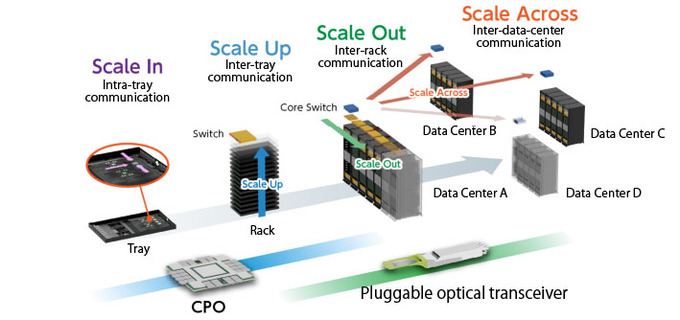
Scale Across: Connecting Multiple Data Centers and Regions
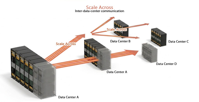
Scale Across is the idea of going beyond the bounds of a single data center or facility to connect AI clusters (computing systems built from multiple coordinated GPUs and servers) distributed across several sites, so that the whole operates in concert as if it were a single data center. It is an area where the distribution and interconnection of data centers—DCI (Data Center Interconnect)—is expected to grow, and it can be divided into two types according to connection distance.
Campus Scale Across
:connections between multiple data centers on the same campus or in relatively close proximity.
Long-haul Scale Across
longer-distance connections between data centers that span metropolitan areas or regions.
In both cases, because the computing facilities at multiple sites are used as a single whole, connections must be fast, high-capacity, and low-latency. Such connections are expected to make use of pluggable transceivers suited to the distance and application.
An optical transceiver is a communication module that converts the electrical signals it receives from network equipment into optical signals for transmission, and converts received optical signals back into electrical signals. Removable, pluggable transceivers are used in a wide variety of connections—not only between data centers, but also between racks and between switches inside a data center. Today, optical transceivers are used most widely in the Scale Out networks within data centers, and they are also expected to be used for the site-to-site connections of Scale Across, depending on distance and application.
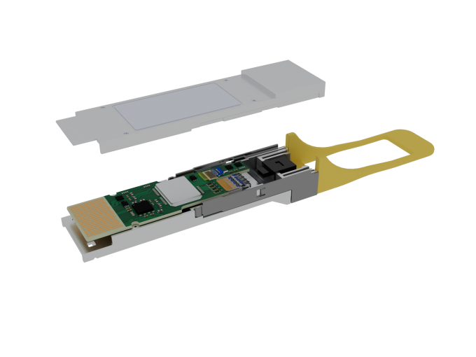
For a detailed explanation of how optical transceivers work and the latest trends, please see our related article: Optical Transceiver Fundamentals and Recent Trends
How Dexerials can address the challenges of this drive toward higher speeds—and with what products—will be covered in a separate article, "Dexerials Products for Scale Across Optical Transceivers."
Scale Out: Adding Servers and Racks to Expand the Scope of Computation
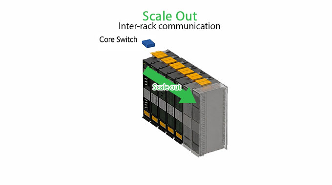
Scale Out is the idea of networking together multiple servers—and computing systems built through Scale Up—to expand the scope of computation within a data center. Because processing is divided across multiple servers, it requires both the communication capacity to move large volumes of data efficiently and mechanisms to keep communication delays low.
In Scale Out, pluggable transceivers are widely used for the connections between servers and racks. As the number of connected devices and the required capacity grow, however, the electrical wiring that links the switch ASIC to the optical transceivers on the front panel becomes longer, making signal loss and power consumption more likely to increase. To shorten this wiring, technologies are being developed that place the point of conversion to light close to the switch ASIC. One of these is CPO (Co-Packaged Optics), which houses the switch ASIC and the optical engine in the same package. By placing the optical engine that converts between electrical and optical signals near the switch ASIC, CPO shortens the distance that high-speed electrical signals must travel. This means that optical communication is expanding into short-reach applications that have traditionally relied on electrical wiring, and adoption of CPO network switches is expected to increase. (The New Optical Interface: Novel Connector Designs and Intelligent Alignments Enable the CPO Era | Features | Feb 2026 | Photonics Spectra)
Development of products that adopt CPO is also progressing. Broadcom has announced the "Tomahawk 6 – Davisson," a 102.4 Tb/s switch that integrates the switch ASIC with an optical engine. (Broadcom Announces Tomahawk® 6 – Davisson, the Industry’s First 102.4-Tbps Ethernet Switch with Co-Packaged Optics) NVIDIA, too, has announced "Spectrum-X Ethernet Photonics" and "Quantum-X InfiniBand Photonics," both of which adopt CPO (NVIDIA,Silicon Photonics Networking for Agentic AI | NVIDIA) The components involved in Scale Out, and the technologies Dexerials can offer, will be covered in a future dedicated article.
Scale Up: Connecting Multiple GPUs to Operate as One Large Computing System
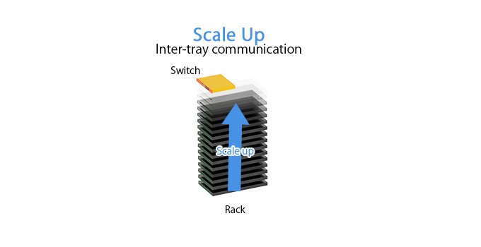
Scale Up is the idea of connecting multiple GPUs, XPUs (a term for compute semiconductors, including GPUs), memory, and other components at high speed so that they operate as a single large computing system. The scope of these connections is not limited to the interior of a single server; it can extend within a rack and across multiple racks.
Copper electrical wiring is widely used today, but as AI scales up, the volume of data that must be sent at once increases and the demands on power consumption grow stricter, making it difficult to keep extending communication distance and speed with copper wiring alone. As a result, development is advancing on technologies that shorten electrical wiring and exchange data using light.
One possible future configuration under study places the optical engine that generates optical signals near the GPU/XPU package and connects GPUs/XPUs to one another with light. The aim is a configuration that shortens the high-speed electrical wiring between GPUs/XPUs and achieves the connection optically.
Development is also progressing toward introducing optical interconnects (technology that uses light to connect equipment and semiconductors) into Scale Up. Marvell has unveiled a 3D silicon photonics optical engine with a 200 Gbps electrical–optical interface for AI clusters. (Marvell Demonstrates Industry’s First 200G 3D Silicon Photonics Engine to Scale Accelerated Infrastructure) NVIDIA has announced "NVLink Fusion," which connects multiple GPUs and custom semiconductors, with partners including MediaTek. (MediaTek | NVLink Fusion | Custom AI ASIC Innovation) The components involved in Scale Up, and where Dexerials can contribute, will be covered in a future dedicated article.
Scale In: Raising Processing Performance Inside the Chip and Package
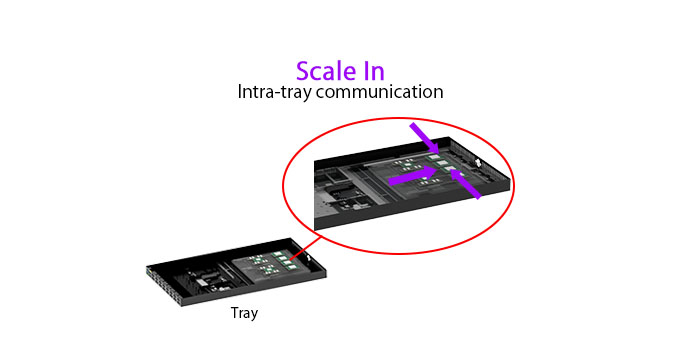
Scale In is the idea of raising processing performance and power efficiency inside a chip, a package, or a single piece of computing equipment. It connects components such as GPUs, HBM (High Bandwidth Memory—high-bandwidth memory placed close to the GPU), and chiplets (small semiconductor chips divided by function) at high density over short distances, enabling high-speed data exchange.
Electrical wiring predominates today, but to increase communication capacity and reduce power consumption, research is also underway on introducing optical I/O (data input and output using optical signals) between dies and between chiplets. The more densely dies (a die is an individual chip cut from a semiconductor wafer) are stacked or arranged side by side, the more that congestion in electrical wiring, signal loss, and heat become challenges even at close range. For this reason, technologies that bring light into the interior of the package are being explored. One such approach provides pathways for light within the interposer—the substrate on which chips are mounted—and carries optical signals through them. A substrate with this kind of optical wiring built in is called a photonic interposer, and configurations using a variety of materials, such as silicon and glass, are being researched.
Technology for bringing optical I/O into Scale In is still centered on research and prototyping, and a timeline for widespread mass production is not yet clear (as of July 2026).
Intel has unveiled a prototype system that mounts an optical I/O chiplet in the same package as a CPU and actually transmits data over it. In the future, this is envisioned as optical I/O technology built into the same package as CPUs, GPUs, and other chips to convert between electrical and optical signals. (Intel Demonstrates First Fully Integrated Optical I/O Chiplet – Intel Newsroom) The components involved in Scale In, and where Dexerials can contribute, will be covered in a future dedicated article.
Summary: Understanding Photonics-Electronics Convergence Through Connection Distance and Role
As we have seen, connections in AI infrastructure can be organized into four perspectives: Scale In, which raises processing performance inside the chip and package; Scale Up, which makes multiple GPUs operate as one large computing system; Scale Out, which adds servers and racks to expand the scope of computation; and Scale Across, which connects multiple data centers and regions. Each differs in the distance and target of its connections and in its role within the system. They do not replace one another in sequence; rather, they are used in combination according to the configuration and purpose of the AI infrastructure.
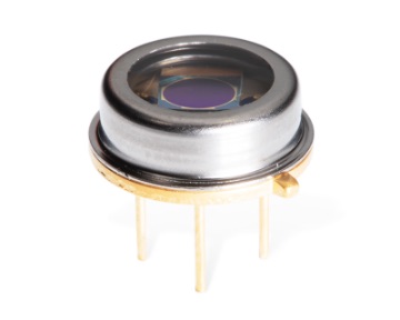
Today, optical transceivers are used most widely in Scale Out within data centers, and their use in Scale Across is expected to expand as well. Scale Up and Scale In still rely mainly on electrical connections, but technology development is advancing to introduce optical interconnects and optical I/O in pursuit of greater communication capacity, lower latency, and reduced power consumption. As this development progresses, the point at which signals convert to light is expected to move closer and closer to the chip. As optical communication reaches a wider range and its conversion points move nearer to the chip, the implementation challenges also change—including optical coupling technology that joins light with low loss, heterogeneous integration technology that bonds different materials and devices with high precision, and high-density packaging technology (part of the broader field of advanced packaging) that supports greater layering and density. Dexerials is working to solve these challenges not only with photodiodes that convert light into electricity (high-speed photodiodes, or PDs) and monitor PDs that monitor and control optical output, but also with industrial adhesives that fix components precisely in place, Anisotropic Conductive Film (ACF) that handles fine electrical connections, inorganic optical devices that control the direction and amount of light, and through the development of new products. Underlying all of these is a common idea: shortening the distance covered by electrical wiring to curb signal loss and power consumption.
In the increasingly prominent field of Photonics-Electronics Convergence, Dexerials will continue to pursue technologies that help solve the challenges engineers face.
Related articles



Dexerials is a materials manufacturer that produces materials essential for the evolution of devices and next-generation solutions.
We will create new value with partners around the world in areas including electronic components, bonding materials, and optical materials.
- Share
We provide materials on our products and manufacturing technologies.
They can be downloaded for free.
Download MaterialsRelated Products

Related articles
Photonics Popular Articles








We provide materials on our products and manufacturing technologies.
They can be downloaded for free.
Download Materials