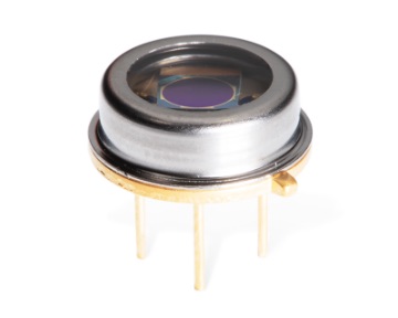
- Optical Semiconductor Products
Development of Waveguide Photodiodes—The Challenge of Speed Enhancement through Integration with UTC-PD (Uni-Traveling Carrier Photodiode)
目次
- 1. New Technology Development Supporting Data Center Evolution
- 2. The Surge in Data Traffic and Limitations of Conventional Photodiodes
- 3. Combining Waveguide Photodiodes with UTC-PD
- 4. Pursuing Ultra-High Speeds through Integration with UTC-PD
- 5. Optimization Using Simulation and Verification with Advanced Manufacturing and Evaluation Facilities
- 6. Pursuing Ultra-High Speeds through Integration with UTC-PD
New Technology Development Supporting Data Center Evolution
In recent years, global data traffic has rapidly increased due to the rapid development of AI technology and the expansion of video streaming services. At the same time, power consumption in data centers has also increased. Considering this situation, from an SDGs perspective, efforts are underway to reduce data center power consumption, with demands for lower power consumption in electronic equipment within data centers, such as servers and switches, as well as individual modules/devices like optical transceivers.
In our previous article, we explained the challenges faced by conventional surface-type photodiodes and the basic structure of waveguide photodiodes that are expected to solve these issues. (You can view "Waveguide Photodiodes: New Technology Supporting Data Center Speed" here.)
In this article, we will introduce the combination of waveguide photodiodes with UTC-PD to further enhance performance, as well as specific initiatives toward practical implementation.
The Surge in Data Traffic and Limitations of Conventional Photodiodes
To help you understand the excellent features of waveguide photodiodes, let’s first explain the structural challenges that conventional surface-type photodiodes faced. The figure below shows a schematic diagram of conventional surface-type photodiodes called pn-type and pin-type.
In surface-type photodiodes, light enters from the top of the component and is absorbed by the light absorption layer, converting it into electrical current. To increase light conversion efficiency, thickening the light absorption layer at the boundary between the p-layer and n-layer is effective.
However, as the layer thickens, the distance that carriers (electrons and holes) that transport electricity must travel increases. As a result, signal processing takes longer, leading to a trade-off that reduces “bandwidth.”
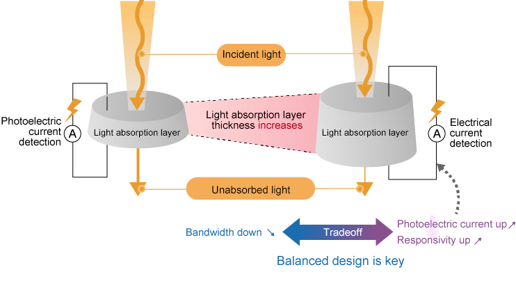
Bandwidth refers to the number of optical signals that can be processed per second. A bandwidth of 1GHz means the ability to process 1 billion signals per second, and the larger the bandwidth, the more information can be processed in a shorter time. In the near future, as data centers require higher speeds, the communication speeds required for client-side optical transceivers are predicted to advance to 400G, 800G, and further to 1.6T and 3.2T.
However, conventional photodiodes faced the dilemma that “increasing sensitivity reduces speed,” limiting performance improvements. This problem has become more serious in recent high-speed communications that require smaller devices. This is one reason why new technologies (waveguide photodiodes and UTC-PD) are needed.
Combining Waveguide Photodiodes with UTC-PD
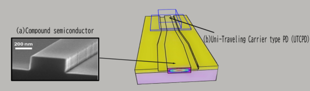
The most significant feature of waveguide photodiodes is that “the direction of light absorption and the direction in which electrical carriers travel are almost perpendicular to each other.” This structure makes it possible to design how much light is absorbed (sensitivity) and how quickly it can be processed (bandwidth) separately.
By combining the light absorption layer in waveguide form with “Uni-Traveling Carrier Photodiode (UTC-PD)” technology, further performance improvements can be expected. Waveguide photodiodes require special techniques for coupling light into tiny waveguide facets, which becomes an important technical point during development.
Pursuing Ultra-High Speeds through Integration with UTC-PD
Another technology to further increase the bandwidth of waveguide photodiodes is the “Uni-Traveling Carrier Photodiode (UTC-PD).” When light hits a semiconductor, its energy creates particles with negative and positive charges—electrons and holes. The movement of these two particles creates current, converting optical signals to electrical signals, which is how photodiodes work.
In conventional pin-type photodiodes, both electrons and holes move in a similar manner to generate current. However, this approach has a significant drawback. Holes move much slower than electrons; Electrons can move at speeds of 100,000 meters per second, holes can only move at less than half that speed. This ‘slow hole’ movement was a major constraint in achieving high-speed optical communications. UTC-PD is an innovative technology designed to solve this ‘slow hole’ problem.
In UTC-PD, the light-absorbing layer is made of P-type semiconductor. P-type semiconductors are created by intentionally mixing special atoms (impurities) into semiconductors to intentionally produce many holes. The majority carriers, holes, can move very quickly as a “group” due to a physical phenomenon called “dielectric relaxation.” It’s like water droplets moving not individually but gathering to form a wave and flowing all at once. This eliminates the problem of slow hole movement.
Additionally, UTC-PD includes a “carrier transport layer” next to the p-type semiconductor light-absorbing layer that doesn’t absorb light. With only electrons playing the main role, it’s also possible to suppress the “space-charge effect” (a phenomenon where the electric field weakens, and output saturates) that occurs when holes and electrons coexist. Imagine conventional pin-type photodiodes as a highway where both fast cars (electrons) and slow cars (holes) share the same lane. This setup can cause traffic jams and inefficiencies. In contrast, UTC-PD is like creating a separate lane for slow cars, allowing fast cars to travel smoothly in their own dedicated lane.
With these structural innovations, UTC-PD enables ultra-high-speed operation exceeding 300GHz and output currents about 10 times larger than conventional pin-Photodiode. By integrating UTC-PD technology with waveguide structures, it is believed that ultra-high-speed and high-capacity signal conversion, essential for next-generation high-speed optical communications, will become achievable. However, to commercialize this technology, several challenges still need to be solved, such as efficiently coupling light into fine waveguides. In particular, how to efficiently guide light into extremely small semiconductor waveguides is a crucial technical point, and we are repeating trial and error to solve this challenge.
Optimization Using Simulation and Verification with Advanced Manufacturing and Evaluation Facilities
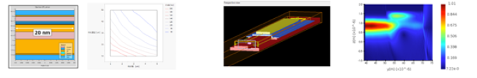
For the practical implementation of waveguide photodiodes, we use computer analysis called “TCAD(Technology Computer Aided Design) simulation” to explore designs that operate at the highest speeds by changing the device structure and materials. We also conduct “FDTD(Finite-Difference Time-Domain) simulation” to explore waveguide coupling efficiency and absorption layer absorption rates, aiming to optimize the structure.
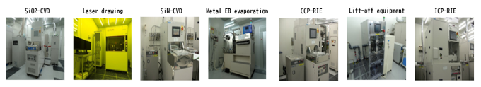
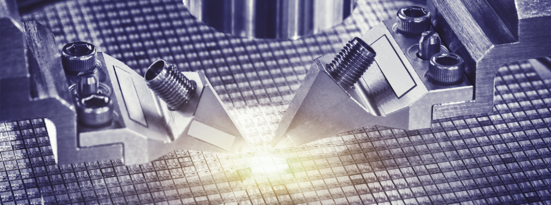
In developing waveguide photodiodes, precise control of the actual manufacturing process is essential in addition to simulation-based optimization. At our company, we are pushing forward with development and mass production using the latest state-of-the-art equipment:
- SiO2-CVD equipment
- Laser drawing equipment
- SiN-CVD equipment
- Metal EB evaporation equipment
- CCP-RIE equipment
- Lift-off equipment
- ICP-RIE equipment
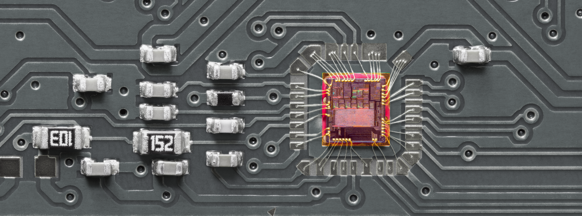
Using these devices for precise manufacturing process control, we are forming waveguide structures and controlling layer thickness.
Pursuing Ultra-High Speeds through Integration with UTC-PD
Currently, Dexerials Photonics Solutions, a consolidated subsidiary of Dexerials, is working on prototypes aiming to achieve bandwidth characteristics exceeding 60GHz, and even beyond 100GHz.
Our development roadmap aims to commercialize 200Gbps/lane waveguide Photodiode by 2026. Looking toward 2030, we also envision developing 400Gbps/lane Photodiode for CPO (Co-Packaged Optics) modules.
Additionally, to achieve lower power consumption, we plan to explore solutions like using optical transceivers without DSP (such as LPO/LRO), moving to Co-Package (CPO) designs, and developing next-generation laser diodes (LD) and modulators.
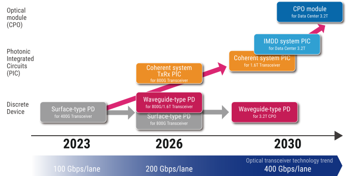
Through these developments, we at Dexerials will continue our research to realize waveguide photodiodes that enable ultra-high-speed optical communications from 400Gbps to further 1.6T and 3.2T.
Related articles


私たちデクセリアルズはデバイスの進化に欠かせない材料や次世代のソリューションを生み出す、マテリアルメーカーです。
電子部品、接合材料、光学材料をはじめと世界中のパートナーと新しい価値を生み出していきます。
- Share
We provide materials on our products and manufacturing technologies.
They can be downloaded for free.
Download Materials関連製品
Related articles
Photonics Popular Articles


We provide materials on our products and manufacturing technologies.
They can be downloaded for free.
Download Materials