- 光半導体関連
フォトダイオードの3タイプとその構造・動作原理
フォトダイオードの3タイプと選定のポイント
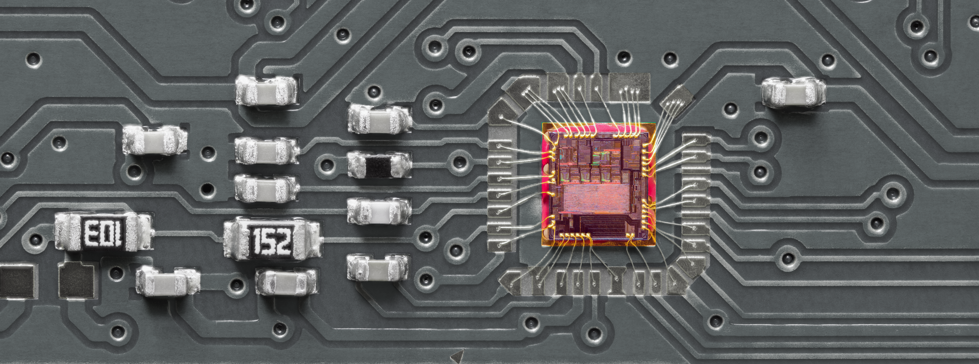
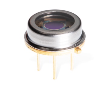
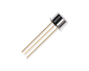
フォトダイオードとは光を電気信号に変換する半導体デバイスです。用途としては、光に反応するセンサや光量計測、DVDなどの光学ディスクの光ピックアップ、光通信における光信号検出など光電変換が必要なさまざまな用途で使われています。フォトダイオードには構造と動作原理の違う、pn型フォトダイオード、pin型フォトダイオード、アバランシェフォトダイオード(Avalanche photodiode:APD)の大きく3つのタイプがあります。本記事では、それぞれの構造と特徴について解説します。
まず、フォトダイオードを解説していくにあたって登場する、受光感度、暗電流(ノイズ)、応答速度の3つの用語について説明します。
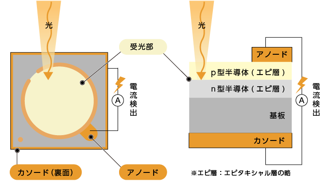
受光感度はフォトダイオードが光をどれだけ効率的に吸収し、電子とホール(正孔)を生成するかを示しています。受光感度が高いほど、生成される電流も大きくなります。
暗電流は、フォトダイオードに光が当たっていない暗闇の状態でも流れる小さな電流のことです。この電流が生成される原因として、外部からの熱によるキャリア(電子やホール)の自然発生や、結晶欠陥や不純物による電子の励起が挙げられます。暗電流はセンサのノイズとなり、測定精度や感度を低下させるため、できるだけ発生を抑える必要があります。
応答速度は、光がフォトダイオードに入射してから、電流が発生して電極から外部に流れるまでの値となり、多くの場合時間で表されます。素子の中の空乏層の厚さ、逆バイアス電圧の大小、デバイスの面積、温度などによって変化します。これにより、半導体内を移動する電子の速度は変化し、それによって応答速度も変わります。
pn型フォトダイオード、pin型フォトダイオード、アバランシェフォトダイオード(APD)は、これらの特性に違いがあり、用途に応じた使い分けが必要です。
pn型フォトダイオードの構造と動作原理
ここからは、それぞれのフォトダイオードの構造と動作原理について解説します。
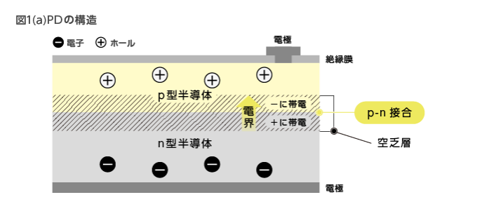
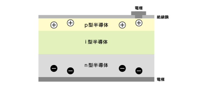
pn型フォトダイオードは基本的な構造のフォトダイオードです。p型半導体とn型半導体を接合し、両端に電極を付けた構造で、太陽電池セルと同じ仕組みとなっています。
pn型フォトダイオードの動作原理について説明します。pn型半導体は、2種類の異なる半導体が接合したことによって、n型半導体の余分な電子がp型半導体に移動し、ホールと結合します。その結果、pn接合付近に「空乏層」と呼ばれる領域が形成されます。空乏層では、n型側が正(+)に、p型側が負(-)に帯電します。すると空乏層の電荷の偏りにより、内部電界が発生します。この内部電界により、pn型フォトダイオードは外部から電圧を加えなくても動作可能となっています。
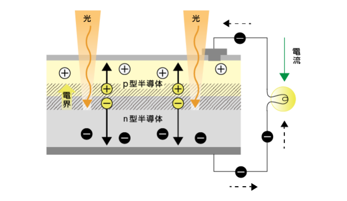
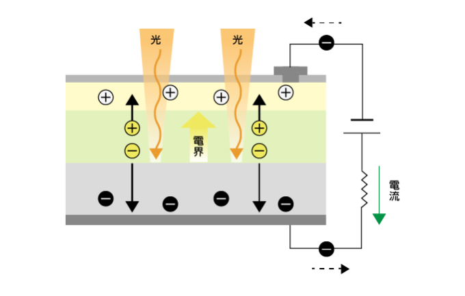
上のイラストのように、pn型フォトダイオードの空乏層に光が入射すると、光のエネルギーによって電子とホールの対が生成されます。その対は内部電界によって、電子はn型半導体側の電極へ、ホールはp型半導体側の電極へと移動します。光を照射している間は、この電子やホールの流れが継続することとなります。
pn型フォトダイオードはシンプルな構造のため、製造が容易でコストが低く、安定動作するという利点があります。また応答速度は遅いものの暗電流が小さいため、光量測定に広く使われます。
pin型フォトダイオードの構造と動作原理
pin型フォトダイオードは、従来のpn型フォトダイオードを改良した構造を持つ光検出器です。その名前が示すように、p型半導体層とn型半導体層の間にi型(Intrinsic)と呼ばれる真性半導体層を挟んだ構造になっています。この設計により、pin型フォトダイオードは高速応答性と高感度を実現しつつ、低い暗電流を維持する優れた特性を持ちます。
従来のpn型フォトダイオードでは、p型層とn型層の接合部付近に自然に形成される狭い空乏層が光を吸収する主な領域となります。一方、pin型フォトダイオードでは意図的に挿入された広いi型層がこの役割を担います。このi層は電子もホールも少ない真性半導体で構成されており、光を効率的に吸収します。
pin型フォトダイオードの動作時には、i型層に逆バイアス電圧が印加されます。これにより、i型層内に強い電界が形成されます。光がi型層に照射されると、光のエネルギーによって電子とホールの対が生成されます。生成された電子とホールは、強い電界の影響を受けて高速で移動します。具体的には、電子はn型層側の電極へ、ホールはp型層側の電極へと移動し、この高速移動が大きな電流を生み出します。
pin型フォトダイオードの主な利点は、高速応答、高感度、そして低暗電流にあります。高速応答は強い電界によるキャリアの高速移動によって実現され、高感度は厚いi型層での効率的な光吸収によってもたらされます。また、i型層の低いキャリア濃度が低暗電流特性に寄与しています。
これらの特性により、pin型フォトダイオードは様々な高性能アプリケーションで広く使用されています。特に、高速データ転送が要求される光通信の受信機や、微弱な信号の検出が必要な医療用イメージング装置などで重要な役割を果たしています。
アバランシェフォトダイオード(APD)の構造と動作原理
アバランシェフォトダイオード(APD)は、従来のフォトダイオードの性能を大幅に向上させた高性能な光検出器です。その最大の特徴は、内部での光電子増倍効果を利用した高感度性にあり、特に微弱光信号の検出に優れています。
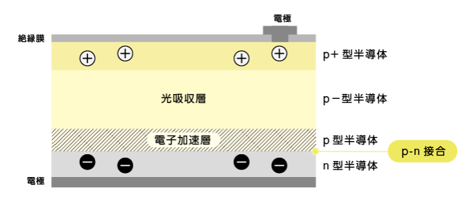
アバランシェフォトダイオード(APD)の構造は、通常のpn型またはpin型フォトダイオードよりも複雑で、主にp型半導体からなる多層構造を持っています。具体的には、p+層、p-層、p層の3層構造となっており、各層が特定の役割を担っています。p+層は高いキャリア濃度をもち、p-層は比較的低いキャリア濃度を持ちます。この構造的特徴が、APDの独特な動作を可能にしています。
アバランシェフォトダイオード(APD)の動作原理は、「アバランシェ増倍」と呼ばれる現象に基づいています。この過程は次のように進行します。
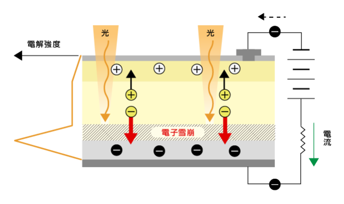
- 光の吸収:p-層が光を吸収し、電子とホールの対を生成します。
- 電子の加速:生成された電子は、強い電界によってp層に向かって加速します。
- 電子の衝突:加速された電子は、半導体の原子と衝突し、新たな電子とホールの対を生成します。
- 連鎖的な増倍:生成された電子も再び加速し、さらなる衝突と電子-ホール対の生成を引き起こします。
- 電子雪崩:この連鎖反応によって、電子とホールの数が雪崩(アバランシェ)のように増加します。
この「電子雪崩」効果により、アバランシェフォトダイオード(APD)は非常に高い感度を実現しています。微弱な光信号でも、内部で大幅に増幅されるため、検出可能な大きな電流となります。
アバランシェフォトダイオード(APD)の動作には高い電圧が必要です。各層にかかる電界は均一ではなく、特にp層を薄くすることで空乏層に大きな電界勾配が形成されます。この強い電界勾配が、効率的な電子雪崩の発生を可能にしています。
アバランシェフォトダイオード(APD)の優れた性能により、光通信システムの受信機や、低照度環境下での天体観測、高感度を要求される科学計測器など、幅広い分野で重要な役割を果たしています。特に、微弱な光信号の検出が必要な場面で、その真価を発揮します。
しかしながら、アバランシェフォトダイオード(APD)にはいくつかの課題もあります。その複雑な構造と高電圧動作の要件により、製造コストが高くなり、他のタイプのフォトダイオードと比べて高価になります。また、適切な動作のためには、温度管理や精密な電圧制御など、より専門的な取り扱いが必要となります。
このように、アバランシェフォトダイオード(APD)は高い性能を持つ反面、使用にはより深い専門知識と適切な運用環境が求められます。しかし、その卓越した感度は、多くの先端的な応用分野で不可欠なものとなっており、光工学技術の発展に大きく貢献しています。
関連記事

私たちデクセリアルズはデバイスの進化に欠かせない材料や次世代のソリューションを生み出す、マテリアルメーカーです。
電子部品、接合材料、光学材料をはじめと世界中のパートナーと新しい価値を生み出していきます。
- SHARE
当社の製品や製造技術に関する資料をご用意しています。
無料でお気軽にダウンロードいただけます。
お役立ち資料のダウンロードはこちら関連製品
関連記事
光半導体関連の人気記事


当社の製品や製造技術に関する資料をご用意しています。
無料でお気軽にダウンロードいただけます。
お役立ち資料のダウンロードはこちら