- Optical Semiconductor Products
The Manufacturing of Optical Semiconductors: Processes and Quality Control
Optical semiconductors are essential components in modern electronics and communication technologies, and their manufacturing processes are both intricate and precise. This article provides a detailed explanation of the manufacturing process of optical semiconductors, highlighting the importance of each step and the stringent quality control measures implemented to ensure the quality of the products.
目次
The manufacturing process of optical semiconductors
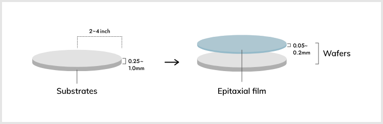
Wafers: The foundation of optical semiconductors
The manufacturing of optical semiconductors begins with the development of a thin film (epitaxial layer) on substrates like gallium arsenide, indium phosphide, gallium phosphide, sapphire, or silicon carbide to form the device’s functionalities. These substrates, with thicknesses ranging from 0.25mm to 1.0mm and diameters from 2 inches (50mm) to 4 inches (100mm), serve as the base for the epitaxial layer, which typically measures between 0.05mm and 0.2mm in thickness. These disc-shaped substrates are referred to as wafers.
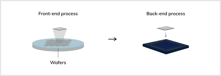
Overview of the manufacturing process (front-end, back-end, and inspection)
The manufacturing of optical semiconductor devices progresses by preparing wafers and sequentially processing them through numerous stages. Generally, the manufacturing process is divided into two main phases: the front-end and the back-end.
During the front-end process, the wafer is processed while still in one piece. In the back-end phase, the wafer is divided into individual chips. Eventually, all the selected chips are incorporated into packages to create the finished product.
Each stage of the manufacturing process includes inspections for quality control. Adhering to procedure manuals, both sampling and total inspections are carried out to manage the processes and quality. This ensures the quality of the products, allowing us to provide customers with reliable optical semiconductor devices.
The front-end process
The front-end process involves a series of steps in which light-emitting or photo-detecting elements are formed directly on silicon or compound semiconductor wafers. The main stages of this process are detailed below:
Elemental function design and pattern design
Here, the functionality and structure of the elements are designed to meet customer requirements. The element’s patterns are designed and then transferred onto a glass substrate to create a photomask.
① Film Deposition
During this stage, insulating thin films such as oxide and nitride are formed on the wafer.
②Photolithography
This involves a series of processes including the application of the photoresist, pattern transfer using a photomask, exposure, and development.
③ Etching
After exposing the photoresist-applied wafer to ultraviolet light, this process involves removing insulating thin films or semiconductor materials from either the masked or unmasked areas.
④ Impurity diffusion
At this stage, specific impurities are introduced into ultra-pure semiconductor wafers, altering their electrical properties. This results in the formation of P/N junctions.
These processes are repeated according to a flow chart, ultimately leading to the formation of elements.
Electrode Formation
In this step, ohmic electrodes are formed. Optical semiconductors have polarity, with the anode as the (+) electrode and the cathode as the (-) electrode. The pattern for electrode formation is transferred using a photomask.
Wafer Inspection
At the end of the manufacturing process, the electrical performance of the wafers is tested using a testing device (prober). This step is also referred to as probe testing or wafer sorting. Every individual element connected to the wafer is examined for any functional imperfections, and if they meet the required specifications, they are classified as ‘good.’
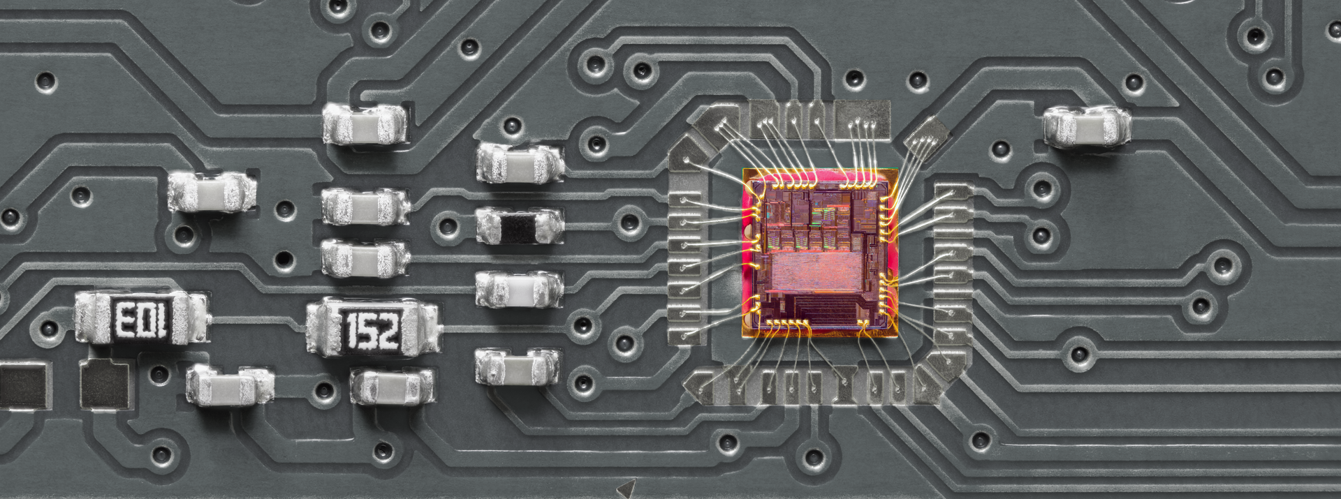
The back-end process
The back-end process consists of four main stages: wafer mounting, die bonding, wire bonding, and packaging.
Water mounting
During this stage, wafers are mounted onto an adhesive plastic tape before being cut into individual pieces. The tape-mounted wafer is then attached to a ring.
Wafer dicing
Here, the wafer containing thousands of elements is sliced into small pieces, known as dies.
Die bonding
During die bonding, the dies are placed onto a package or substrate and affixed using materials like Ag paste. This process is also known as die attachment.
Wire bonding
This stage involves connecting the die to the external package or substrate. A combination of heat, pressure, and ultrasonic energy is used to weld wires on both sides.
Visual inspection
The placement of the dies, the condition of the epoxy paste, and the wiring are inspected visually.
Packaging
During this step, the dies are sealed with materials like silicon or epoxy plastics to protect them from physical damage and chemical corrosion. The term ‘encapsulation’ is often used interchangeably with packaging.
Finished product testing
After completing the back-end process, the optical semiconductor devices undergo various electrical tests to determine if they function correctly. The proportion of devices that pass performance testing is referred to as the yield.
Through these consecutive stages, the manufacturing of optical semiconductor devices is completed. Each stage requires precision and meticulous work, resulting in the production of high-quality optical semiconductor devices.
Optical Semiconductor Manufacturing System at Dexerials
Dexerials Photonics Solutions Corporation, a subsidiary of Dexerials Corporation, manufactures high-quality optical semiconductors. We ensure the quality and performance of our opto-semiconductor devices through thorough product quality control.
Our front-end process starts at the Eniwa Plant in Eniwa City, Hokkaido, Japan, from the development stage. This system ensures product quality and performance, while also improving production efficiency.
The Eniwa Plant continues to handle the post-processing, and some of it will be transferred to the Kamisunagawa Plant in Kamisunagawa-cho, Sorachi-gun, Hokkaido. Kamisunagawa Plant specializes in mass production, where cost reduction and mass production are pursued. This allows us to provide our customers with products that have high cost performance.
Dexerials Group Inc, with Dexerials Photonics Solutions Corporation at its core, will continue to evolve and maintain its position as a leading manufacturer of optical semiconductor devices through these efforts.
Related articles

私たちデクセリアルズはデバイスの進化に欠かせない材料や次世代のソリューションを生み出す、マテリアルメーカーです。
電子部品、接合材料、光学材料をはじめと世界中のパートナーと新しい価値を生み出していきます。
- Share
We provide materials on our products and manufacturing technologies.
They can be downloaded for free.
Download MaterialsRelated articles
Photonics Popular Articles


We provide materials on our products and manufacturing technologies.
They can be downloaded for free.
Download Materials