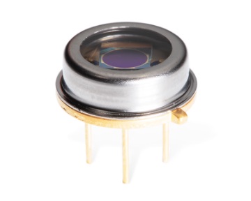
- Optical Semiconductor Products
Design Optimization and Recent Trends in Photodiodes for Communication Applications
目次
Primary characteristics of photodiodes for communication applications
The photodiodes for communication applications used in optical transceivers require designs with materials and structures optimized for each application and purpose. This article will discuss the fundamentals of these designs.
Photodiode performance is largely determined by dark current, responsivity, capacitance, and bandwidth. We will start by explaining these basic building blocks of photodiode design. It is important to note that in actual design, tradeoffs must be made to reach the desired balance between these conflicting factors in performance.
- Dark current (symbol: I d)
Dark current is a small electric current that is generated when no light is falling on the photodiode. Primarily caused by heat or leakage currents, it is a major cause of noise and directly impacts device performance. Because it directly affects the signal-to-noise ratio, dark current levels should be minimized. While reduction is possible through material selection, manufacturing process optimization, and lower operating temperature, there is a tradeoff with responsivity and designs with smaller dark current are less responsive as well. Dark current is a particularly important parameter in use cases that require high responsivity and low noise, and is used as an indicator of device quality and performance. - Responsivity (symbol: R)
The responsivity of a photodiode is the ratio of electrical current output to the intensity of incident light. High-responsivity devices generate large electrical current even with weak light, but noise may increase as well. As a result, it is important to select an appropriate level of responsivity for the specific use case. In particular, there is a tradeoff between responsivity and bandwidth in PIN photodiodes. High-responsivity designs are well-suited for detecting weak signals, but in situations that require fast response it is necessary to balance responsivity and bandwidth. Responsivity design must be done appropriately and carefully based on the requirements of the application. - Capacitance (symbol: C, Cs, Cp)
The capacitance of a photodiode is its ability to store electric charge within the device. This parameter has a major impact on response speed and responsivity. High capacitance slows response speed, but low capacitance can reduce responsivity. It is important to keep capacitance low for applications that require fast response speed, but it is necessary to carefully consider the tradeoff with responsivity. Photodiode capacitance is affected by the width of the device’s light absorption layer and the aperture size. Capacitance is used in bandwidth calculations as well—it is possible to estimate bandwidth using the measured value. - Bandwidth (symbol: BW)
The bandwidth of a photodiode is the range of frequencies of light that it can convert into electrical signals. The higher the bandwidth, the faster the response to signal changes. This enables high-speed operation, but excessively high bandwidth can affect other aspects of performance. Consistency with other components is important in an optical communication system, and it is necessary to choose an appropriate bandwidth based on the needs of the overall system. There is a tradeoff between bandwidth and responsivity in PIN photodiodes, making it important to balance them depending on the application. Appropriate bandwidth design is a key element in optimizing a system’s performance and reliability.
Key points in optimizing designs for higher speed
Here, we will discuss the key points in optimizing photodiode design.
First, we will look at the relationship between bandwidth and capacitance. The higher the bandwidth of a photodiode, the faster it can operate. How, then, should capacitance be designed to increase bandwidth? This is shown in the formulas below.
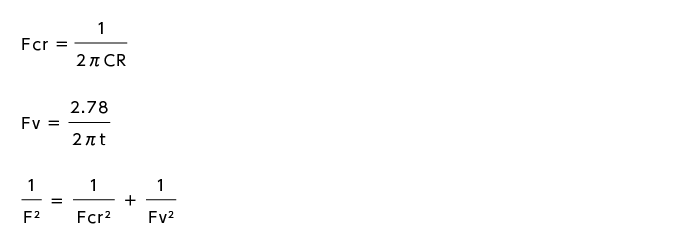
The bandwidth F is calculated based on bandwidth Fcr (derived from capacitance C and resistance R) and bandwidth Fv (derived from time “t” it takes for carriers in the photodiode to flow out as current).
These formulas show the following two key points for high-speed design.
・
Lowering capacitance C
・Shortening carrier transit time t
In photodiode design, it is important to optimize these values.
Next, we will look at ways to lower capacitance C.
The capacitance of a PIN photodiode device depends on the thickness and shape of the PIN junction in the active area.
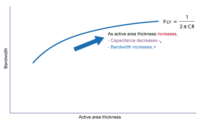
The graph above shows an example of bandwidth calculated based on device capacitance. In a PIN photodiode, as the primary active area (the I-layer) gets thicker, the distance between the P and N layers grows. This reduces the amount of electric charge that can be stored, lowering the photodiode’s capacitance. As capacitance is lowered, bandwidth increases. Bandwidth is the range of frequencies for which the device can operate effectively.
Why does bandwidth increase when capacitance decreases? Imagine you are pouring water in and out of a bucket. This takes time with a large bucket (high capacitance) but is faster with a small bucket (low capacitance). This means it’s possible to process faster signal changes, leading to higher bandwidth.
How to shorten carrier transit time t
Next, how can we shorten carrier transit time t in a PIN photodiode?
Carrier transit time t can be calculated with the following formula.
t =
d
v d
- d: i-InGaAs layer thickness (carrier transit distance)
- v d: vcarrier transit speed (using the theoretical value for transit speed from research papers, etc.)
From this formula, we can see that reducing the thickness of the I-layer (the carrier transit distance) will shorten carrier transit time.
On the other hand, carrier transit time t is inversely proportional to bandwidth.
The graph below shows an example of bandwidth calculated based on carrier transit time.
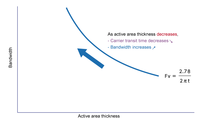
As the active area gets thinner (and the carrier transit time gets shorter), the bandwidth increases. As seen in the bucket example above, when electrons and holes spend more time in transit, the photodiode is slower at following changes in frequency.
The relationship between responsivity and bandwidth
Next, we will examine the relationship between responsivity and bandwidth.
Responsivity and bandwidth are extremely important elements in photodiode design. There is a tradeoff between the two, forcing designers to find a careful balance.
To heighten responsivity, the light absorption layer is made thicker. This allows it to capture more light and convert it into more electrical signals.
However, a thicker light absorption layer means that generated electrons and holes (carriers) must travel a longer distance. This increased transit time limits bandwidth (response speed to signal changes).
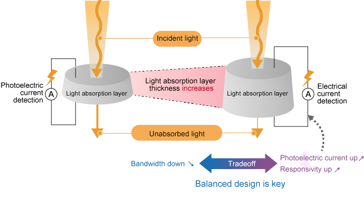
Designers must adjust these elements to optimize photodiodes for the intended application. They may prioritize responsivity when detection of weak light is important and emphasize bandwidth for high-speed communication.
As seen above, the various elements in a photodiode are like the ends of a balance scale—raising one side means the other will go down. The key to photodiode design is to consider these tradeoffs and find the optimal balance for the specific application.
For many years, the Dexerials Group has developed, manufactured, and sold photodiodes for various wavelengths including ultraviolet, infrared, and visible light. Please consult with us any time so we can use our rich experience to select the optimal photodiodes for your needs.
For details on how to select photodiodes, please refer to this article.
Related articles

私たちデクセリアルズはデバイスの進化に欠かせない材料や次世代のソリューションを生み出す、マテリアルメーカーです。
電子部品、接合材料、光学材料をはじめと世界中のパートナーと新しい価値を生み出していきます。
- Share
We provide materials on our products and manufacturing technologies.
They can be downloaded for free.
Download Materials関連製品
Related articles
Photonics Popular Articles


We provide materials on our products and manufacturing technologies.
They can be downloaded for free.
Download Materials