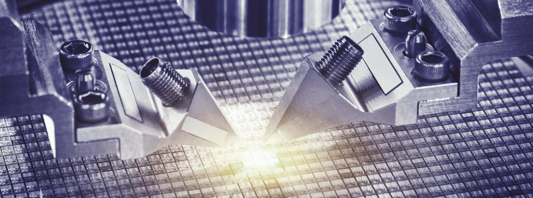
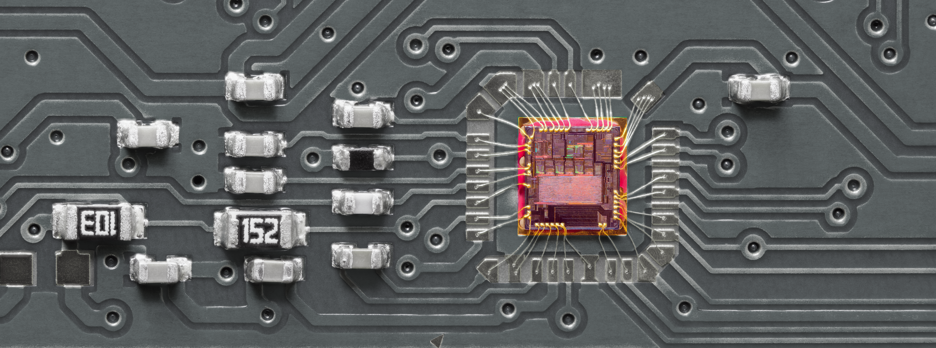
- 光半導体関連
導波路型フォトダイオードの仕組み―データセンターの高速化を支える新技術
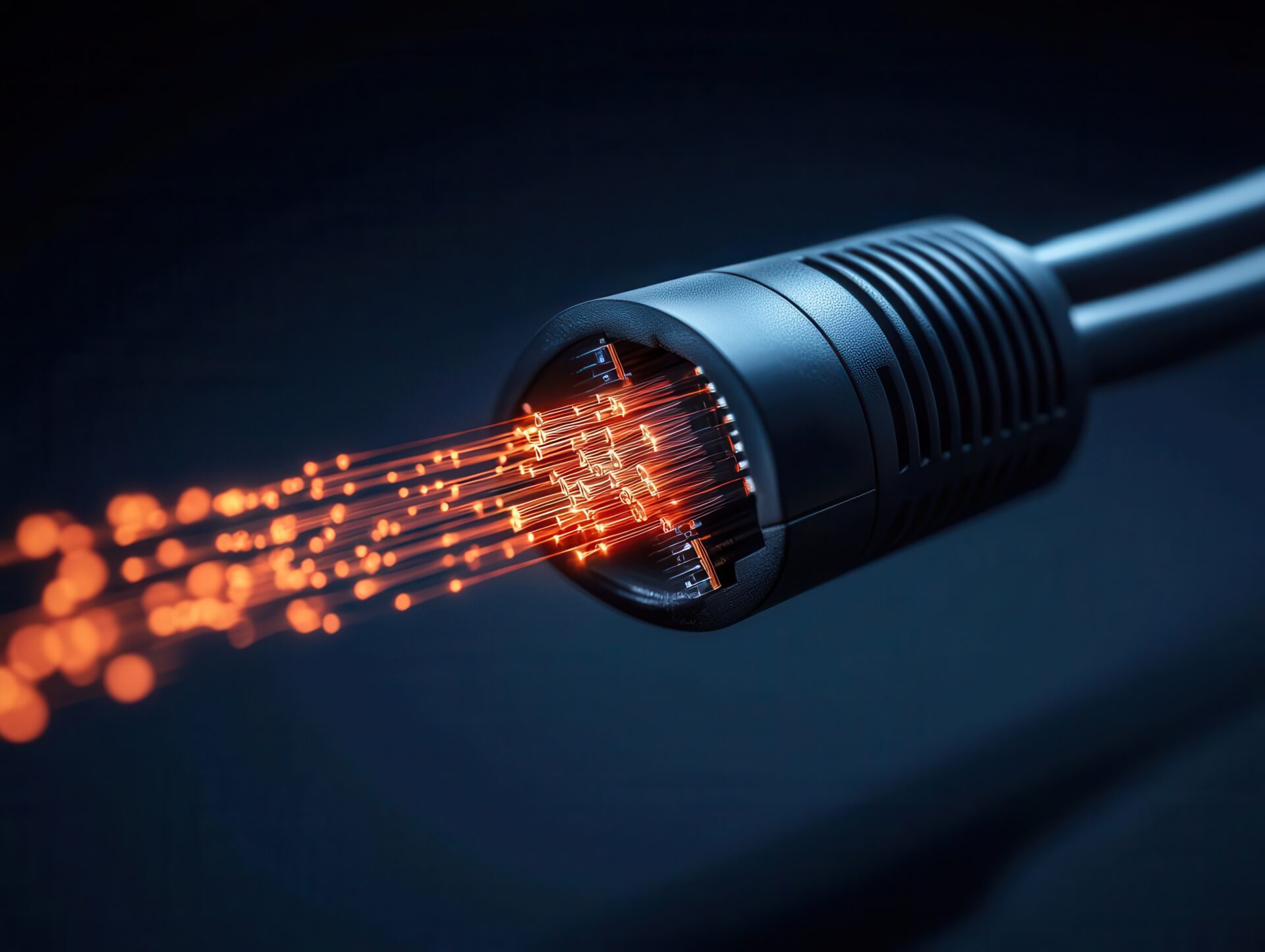
データセンターの高速化と光トランシーバーの進化
近年、世界中でデータセンターを経由するトラフィックの量が、大きく増加しています。AI/ML(人工知能/機械学習)の開発・実用化の拡大、クラウドサービスの普及、映像配信サービスやAR/VRなどのコンテンツの充実と利用人口の増加により、データトラフィックは今後も増大を続けることが確実視されています。このような状況に対応するため、基幹系の光通信ネットワークにはさらなる大容量化・高速化が求められています。
光通信を使ったサービスを安定的にユーザーに提供するためには、インフラネットワーク・データセンター内のネットワークの高速化・低遅延化が必要になります。そのカギを握るのが、「光トランシーバー」と呼ばれる部品の対応速度です。これまでの光トランシーバーの速度は100Gbpsが一般的でしたが、ネットワークの高速化要求に伴い、2024年ごろから400G、800Gの高速な製品が市場に導入され始めています。さらに今後、光トランシーバーに求められる速度は、1.6T、3.2Tbpsと進んでいくことが予測されます。
フォトダイオードの基本構造と課題
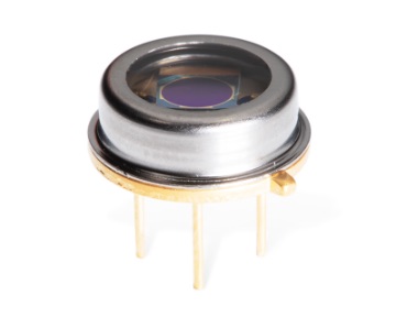
光トランシーバーは、電気信号と光信号を相互に変換する装置です。送信部では半導体レーザーダイオードが電気を光に変換し、受信部ではフォトダイオード(PD)が光を電気に変換します。光トランシーバー内では、これらの部品が連携して高速なデータ通信を実現しています。
フォトダイオードの基本的な構造や動作原理については、こちらの記事で詳しく解説していますが、本記事では特に高速化における課題に焦点を当てて説明します。
導波路型フォトダイオードも、光ファイバーを通じて伝わる光信号を電気信号に変換する装置です。その名前の通り、光を導く「導波路」という通り道と、光を電気に変換する「フォトダイオード」を組み合わせた部品になります。従来のフォトダイオードと導波路型フォトダイオードの大きな違いは、その「構造」にあります。
下図は、一般的なフォトダイオード(pn型)の構造です。
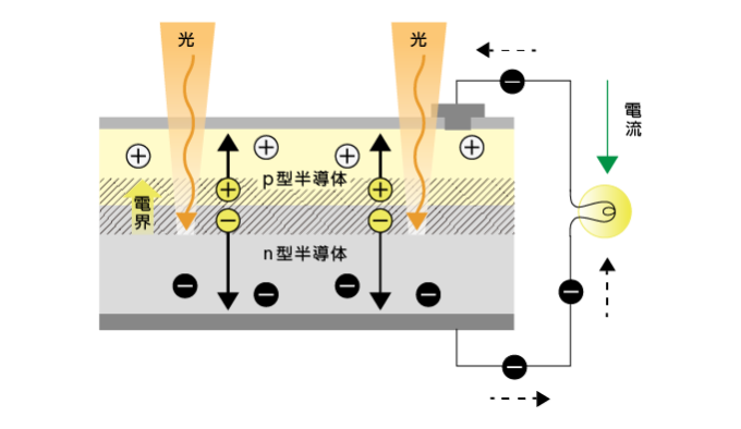
従来のpn型フォトダイオードは、正孔(プラスの電荷を持つ粒子)が多いp型半導体の層が上部にあり、マイナスの電荷を持つ電子が多いn型半導体層が下部にある構造です。その接合部には「空乏層」と呼ばれる層ができ、主にその付近で光が吸収されます。
pn型フォトダイオードは、構造がシンプルなため製造が比較的容易です。しかし、その構造ゆえに高速化が難しいという課題がありました。
フォトダイオードの高速化において重要なのは「帯域幅」です。帯域幅は1秒間に処理できる信号の回数を表し、これが大きいほどより多くの情報を短時間に処理できます。例えば、帯域幅が1GHzであれば1秒間に10億回の信号処理が可能となります。
pn型フォトダイオードでは、光を効率よく吸収するため、光を吸収する領域(空乏層)を厚くする必要があります。これは、半導体内部を光が通過する距離が長いほど、より多くの光を吸収できるためです。しかし空乏層を厚くすると、光によって生成された電子と正孔の移動距離が長くなるため、デバイスの応答速度が遅くなるという問題が生じます。
導波路型フォトダイオードの革新的な構造
この問題を解決するために考案されたのが、新しい構造を持つ「導波路型フォトダイオード」です。導波路型フォトダイオードは、光の吸収とキャリアの移動を効率的に行える設計となっており、高速性と高感度を両立させることができます。
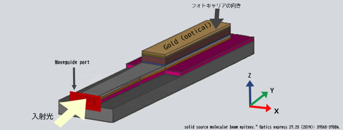
従来のフォトダイオードは、光が部品の上側から入射し、空乏層など光を吸収する半導体層がその光を吸収して電気に変えます。これに対して、導波路型フォトダイオードでは、光が横から入ってきて、「導波路」と呼ばれる化合物半導体でできた横に長い層の中を通りながら徐々に吸収され、電気に変わります。
これは、従来型のフォトダイオードは雨が真上から地面に降り注ぐイメージなのに対し、導波路型は長い水平な管の中を水(実際には光)が流れていくイメージです。この横方向の光伝搬という特徴により、光が吸収層内を伝搬する距離を数十から数百マイクロメートルと長く取ることができるため、光の吸収効率を大幅に向上させることができます。また、導波路の層を薄く作れる特徴も重要です。薄い導波路層により、光によって生成された電子や正孔が電極まで移動する時間が短くなり、高速な応答が可能になります。さらに、デバイスを薄く作れることから、他の光部品と同じ基板上に集積化しやすく、部品の小型化にもつながります。
このように、導波路型フォトダイオードは、光の吸収効率と応答速度の両方を高いレベルで実現可能な技術です。ただし、微細な導波路に光を効率よく結合させる技術など、実用化に向けてはまだいくつかの課題があります。これらの課題解決に向けた取り組みや、より詳しい応用例については、続編の記事でご紹介しています。
私たちデクセリアルズは、導波路型フォトダイオードの開発を通じて、次世代の高速光通信の実現に取り組んでまいります。
関連記事


私たちデクセリアルズはデバイスの進化に欠かせない材料や次世代のソリューションを生み出す、マテリアルメーカーです。
電子部品、接合材料、光学材料をはじめと世界中のパートナーと新しい価値を生み出していきます。
- SHARE
当社の製品や製造技術に関する資料をご用意しています。
無料でお気軽にダウンロードいただけます。
お役立ち資料のダウンロードはこちら関連製品
関連記事
光半導体関連の人気記事


当社の製品や製造技術に関する資料をご用意しています。
無料でお気軽にダウンロードいただけます。
お役立ち資料のダウンロードはこちら