- 接合関連
異方性導電膜(ACF)の新用途―スマホ・タブレットPCのカメラ、車載カメラ、防犯用カメラ
目次
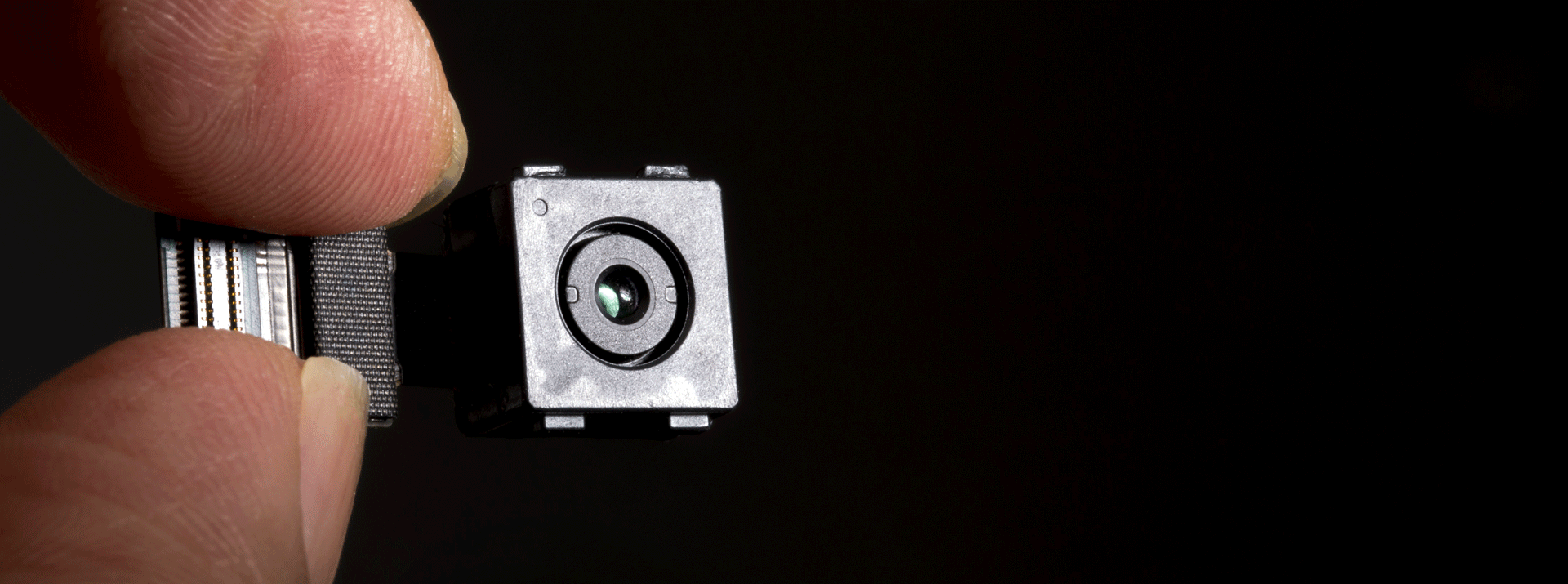
異方性導電膜(ACF)の主な用途 カメラモジュール部品の組み立てに活躍
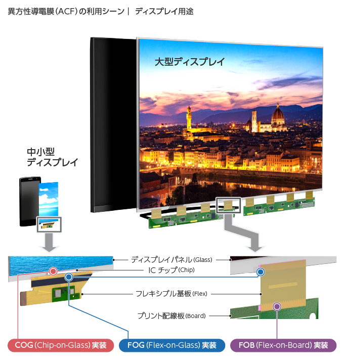
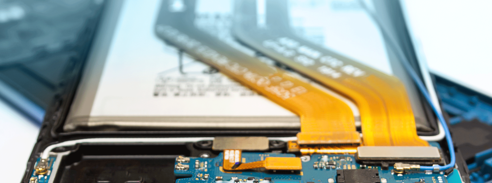
異方性導電膜(以下、ACF)は、ICなどの電子部品を回路基板に固定し、電気的に接続するフィルム形状の接合材料です。フィルム状の熱硬化性樹脂のなかに、導電性の粒子が分散して含まれ、熱と圧力を加えることで導電粒子が互いの端子間に挟まれ回路が接続されます。ACFは単体で「接着」「導通」「絶縁」の機能を発揮することから、従来のはんだ接続やコネクター接続を代替する実装材料として、用途が広がっています。とくに微細化した配線を同時に接続する「ファインピッチ接続」が必要なディスプレイ、低温での接続が必要なタッチパネル、ICカードなどの電気回路の接続に活用されてきました。

なかでも近年、スマートフォンやタブレットPCのカメラ、車載カメラや防犯用カメラなどに搭載される、カメラモジュール部品での接合にもACFが使われています。本記事では、カメラモジュールでの接合に使用されるACFの特長について解説します。
異方性導電フィルム ディスプレイ用とカメラモジュール用の違い
カメラモジュールの特長の一つに、ディスプレイ等に比べて接合する端子の数が少ないことが挙げられます。大画面テレビや大型化しているディスプレイでは、画素数の増加にともなってACFで接合する端子の数も増え、製品によっては1台で数千もの端子を同時に接続します。それに比べてカメラモジュールの端子は数十と少なく、また個々の端子の面積も大きいところです。
この他、実装材料としてのACFにもディスプレイ用と大きく違う点があります。それは、「導電」の機能を発揮するためにACFに含まれている導電粒子が、直径約20μmと比較的大きな粒子であることです(ディスプレイ用のACFに含まれる導電粒子は数ミクロン程度)。
その理由は、ディスプレイのガラス基板に比べて、カメラモジュールで使用される部品や基板の実装部はガラスやICほど平坦でないためです。使用する部品の構造や大きさにもよりますが、実装部の平坦度が20ミクロンを超えるような歪みを持つ部品も存在しています。
大径導電粒子で基板の歪みによる接続の難点を解消
ディスプレイで使用されるガラスに比べてセラミック製の回路基板やプリント配線板の歪みが大きいのは、製法の違いが理由です。ディスプレイのガラス基板は単層で、液状の原料を固化させて作るため、表面は非常に高いレベルで平板になります。一方セラミック基板などの多層構造を持つ回路基板は、熱的・機械的特性の異なる複数の層を積層・一体化させており、どうしても歪みが発生します。特にセラミック基板の場合は「焼成」と言われる焼き固める工程で瀬戸物のように収縮するため、比較的大きな歪みが発生します。加えて、カメラモジュールの場合、センサー部をよけるための窓のような空間が必要で、これも歪みを助長する要因となっています。
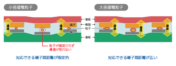
ACFは回路を接続する際に、下記のイラストのように対向する端子と端子の間で導電粒子が挟まれて潰れることで導通をとります。小さな径の導電粒子を、圧着部が平坦でない基板に用いた場合、左図の真ん中の端子のように、粒子が潰れずに導通が取れなくなる可能性があります。そのため、カメラモジュールの組立に使用されるACFは、従来のディスプレイ用ACFよりも大径の導電粒子を採用しています。
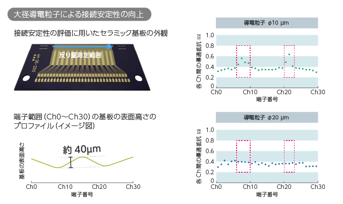
デクセリアルズでは大径導電粒子の効果を検証するために、およそ40μmの歪みを持つセラミック基板と導電粒子径の異なる2種類のACFを準備しました。下記の2つのグラフは、上側が直径約10μmの導電粒子、下側が約20μmの導電粒子を含むACFで回路を接続したときの、回路一つひとつの「抵抗値」を示しています。上のグラフを見ると、赤い点線で囲んだ部分が高くなっていますが、それはすなわち、回路がうまく接続できていないことを意味しており、基板の歪みの傾向ともおおよそ一致しています。それに対して下側のグラフは、どの端子もほぼ同じ抵抗値となっており、基板に歪みがあっても正常に導通がとれていることがわかります。
低圧で接合できるメリット
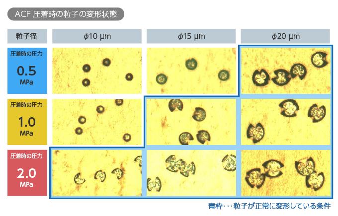
また、大径粒子を採用したACFの優れた特性の一つに、「低圧で接合ができる」ことがあります。カメラの性能はスマートフォンを語る上で欠かせない性能で、高性能化と同時に広角や望遠などデジタル一眼レフカメラ顔負けの進化を遂げています。これらのカメラは非常に精密に出来ており、カメラモジュールの組立では、カメラ本体に不要な力が加わることを嫌って、ACF接合においてもより低圧で接合できることが求められます。
粒子が大径になるほど少ない力で変形し、潰れるため、小さな圧力で導通をとることができます。下記は、10μm、15μm、20μmの導電粒子に0.5MPa〜2.0MPaの圧力をかけたときの拡大写真です。径が大きくなるほど少ない圧力で変形していることが確認できます。
以上、カメラモジュールの組立に使用される大径導電粒子を採用したACFの特長についてご説明しました。近年、カメラはスマートフォンをはじめとする様々なエレクトロニクス製品に搭載されており、またこれからは自動車のセンシング用のカメラの需要が飛躍的に伸びていくと考えられており、カメラモジュール用ACFの活躍の場はさらに広がっていくと私たちは予想しています。
関連記事


私たちデクセリアルズはデバイスの進化に欠かせない材料や次世代のソリューションを生み出す、マテリアルメーカーです。
電子部品、接合材料、光学材料をはじめと世界中のパートナーと新しい価値を生み出していきます。
- SHARE
当社の製品や製造技術に関する資料をご用意しています。
無料でお気軽にダウンロードいただけます。
お役立ち資料のダウンロードはこちら
関連記事
接合関連の人気記事


当社の製品や製造技術に関する資料をご用意しています。
無料でお気軽にダウンロードいただけます。
お役立ち資料のダウンロードはこちら