- Bonding Products
New trends and applications of ACF technology
Contents
New particle-arrayed ACFs for camera applications
Anisotropic Conductive Film (ACF), developed in 1977 by Dexerials’ antecedent company, was the world’s first film material made for electronic circuit connections. ACF consists of conductive particles, dispersed in a thermosetting resin. It connects pads when heat and pressure are applied.
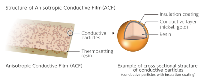
In December 2020, Dexerials announced the launch of a new ACF series, ‘Particle-Arrayed ACF for Camera Modules.’ One of the products, “PAF50C6,” enables the miniaturization of pad bonding in camera modules and touch panels while ensuring reliable connectivity.
Camera module ACFs with large diameter conductive particles
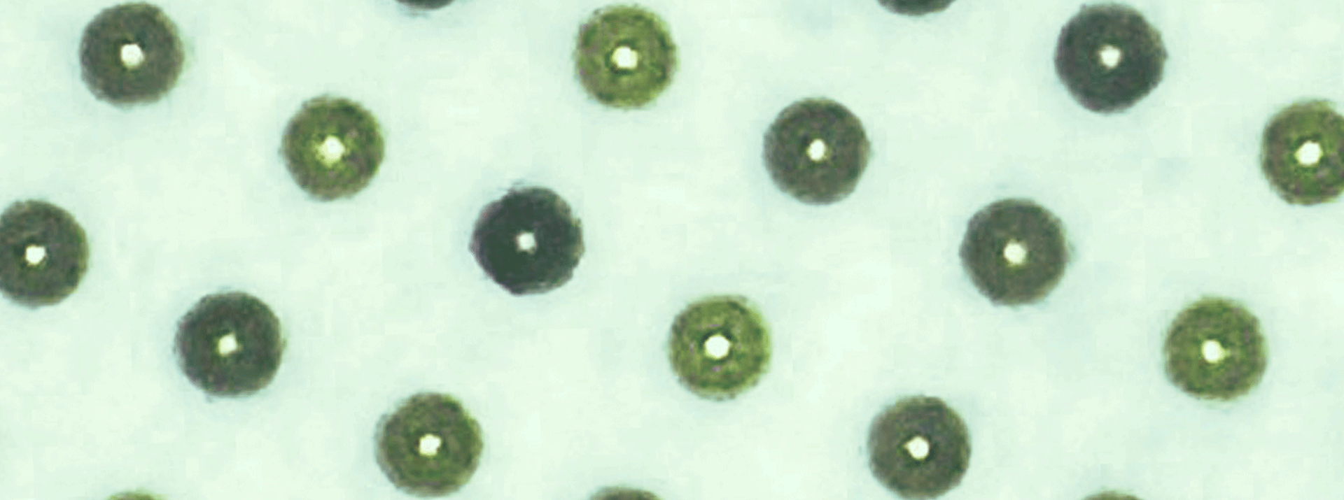
Below is a magnified image of the newly developed Particle-Arrayed ACF for camera module applications on the left and the conventional ACF, PAF300C, used in display connections, on the right. As shown, the particle diameter of the camera module ACF on the left is larger.
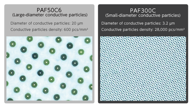
Conductive particles in camera modules are larger because:
1. The spacing between adjacent bonded pads is wider than those in displays, and does not require fine connections.
2. The distortion and unevenness of the adherend, circuit board (ceramic substrate or printed circuit board), is larger than that of glass substrates used in displays.
Below is a diagram showing how ACF particles connect opposing pads. The left structure with small diameter conductive particles shows that the middle pad is not conductive due to the distance variation between pads. However, the structure on the right with large diameter conductive particles allows connection between pads over a wider distance than on the left.
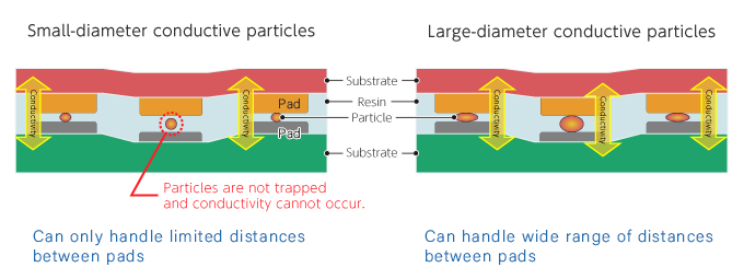
The reason for arraying large diameter conducting particles
Why is it necessary not only to increase the size of the conductive particles in camera module ACFs, but also to arrange them evenly at targeted positions? The main reasons are performance enhancement and miniaturization requirements of camera modules used in smartphones and other devices.
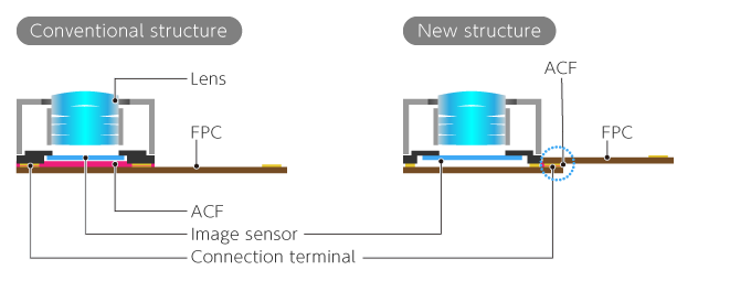
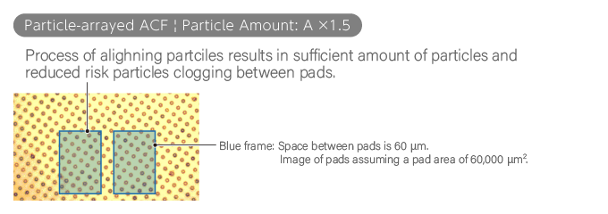
The figure below shows the cross section of the conventional camera module structure on the left and the latest camera module structure on the right. As smartphones become more functional and demand for higher image quality increases, the space available for camera modules continues to shrink to create room for larger sensors. Therefore, the ACF pad bonded areas are being pulled outward, reducing the connection area from 120,000μm2 to about 60,000μm2, half the size previous structures offered.
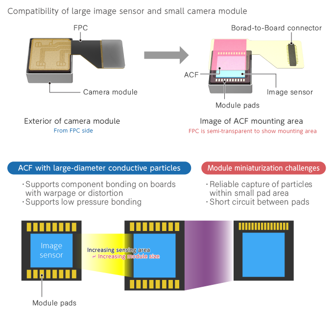
Below is a photo of the dispersed particles in the conventional ‘particle dispersed’ ACF with large diameter conductive particles used for camera modules. The area within the blue frame illustrates the size and arrangement of the pads. Conductive particles in the ACF are sandwiched between the pads by heat and pressure, creating electrical conductivity between the opposing pads. In case of dispersed ACF (1) with large diameter conductive particles density A [pcs/mm2], there are fewer particles trapped between pads, which may result in higher electrical resistance.
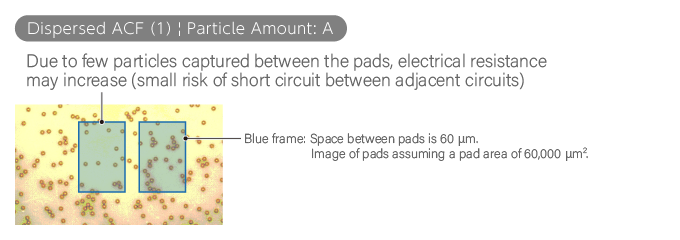
The next image shows the dispersed ACF (2) with 1.5 times as many conductive particles as in the previous dispersed ACF (1). The number of dispersed particles was increased to obtain sufficient conductivity. However, there are areas where the particles are stuck together between pads, increasing the possibility of a short circuit between adjacent pads.
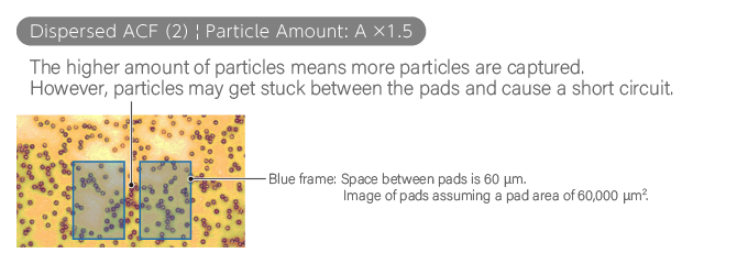
Lastly, below is an photo of the dispersed particles of the newly developed particle-arrayed ACF with aligned large diameter particles. The number of arranged particles is sufficient to obtain good conductivity. The particles are also aligned so that they are not in contact with each other, minimizing the risk of a short circuit. Aligning the particles reduces the bonding area and pad spacing, making it possible for miniaturization of camera modules.
Further application of the technology: Background of pre-cut ACFs
The new large diameter particle-arrayed ACF, developed in conjunction with evolution of the camera module design, demonstrates how ACF technology advances in accordance with the market and new application needs. Another example of it is the “pre-cut ACF,” which was commercialized in December 2021.
Pre-cut ACF is ACF film that is converted into a shape that matches the board and layout of the pads. Bonded pads in displays are often arranged in an elongated rectangular shape, thus making the long tape-shape of conventional ACFs convenient. However, in camera modules, bonded pad surfaces are often not uniform, and there is no need to connect them entirely. The design examples below show how ACFs can be converted depending on the design of the camera module.
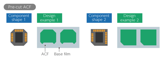
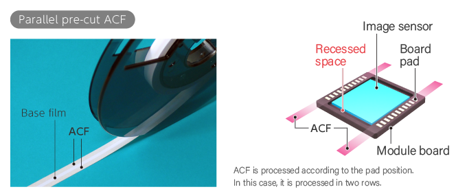
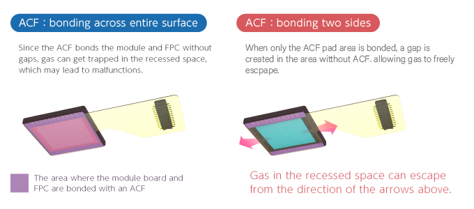
The development of this product stems from a concern when a conventional tape-shaped ACF is used to bond components over an entire surface during assembly of camera modules. After bonding, the water vapor and other gases trapped in the recessed space are not be able to escape. It usually causes problems during module reliability tests such as a PCT (pressure cooker test).
The above mentioned concern is resolved by applying the ACF only to specific areas without bonding the entire pad surfaces. Hence, there is no need to seal the space inside the circuit board. In the example on the right of the graphic below, by applying only two pieces of ACF, gas can escape through the gaps while conductivity is still maintained between the bonded pads.
Dexerials will continue to further improve ACFs to meet various needs of customers.
- SHARE
 Back to top
  Contact us


