- Bonding Products
Achieving innovative Micro LED displays: the particle-arrayed Anisotropic Conductive Film (ACF) ArrayFIX
Contents
What are Micro LED displays?
The Micro LED display is a display technology that is drawing the attention of electronics manufacturers around the world. After many years in research and development, the technology has entered the commercialization phase and is expected to spread at a rapidly increasing pace. This article will explore the basic characteristics of the Micro LED display, the newest trends, and the challenges it faces. It will also explain in detail the changes that ArrayFIX, a particle-arrayed ACF product from Dexerials, can bring to Micro LED display technology.
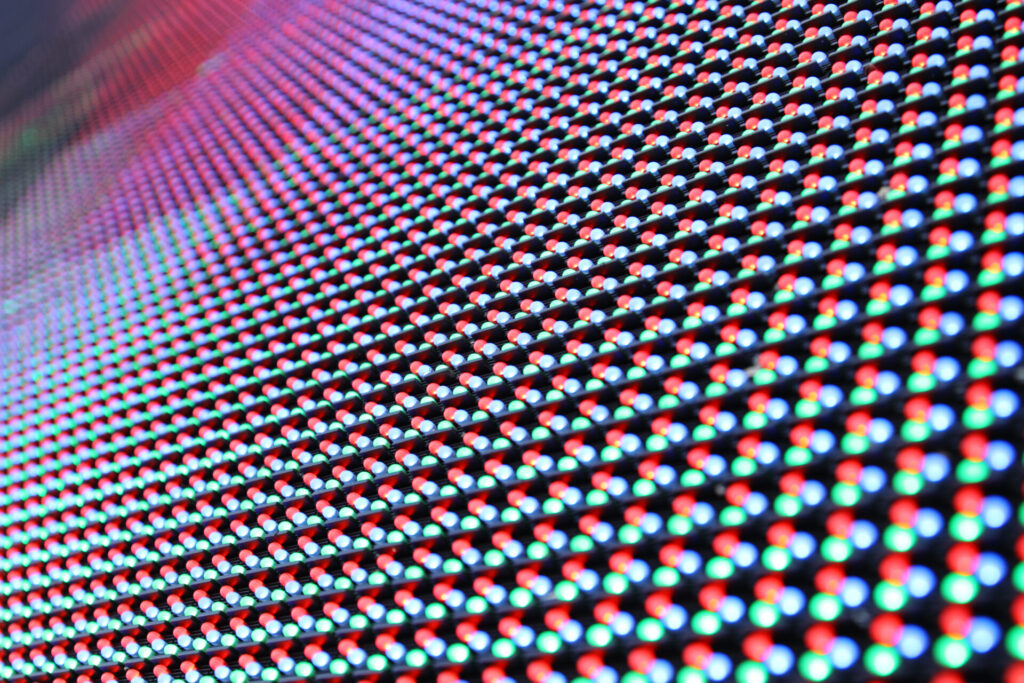
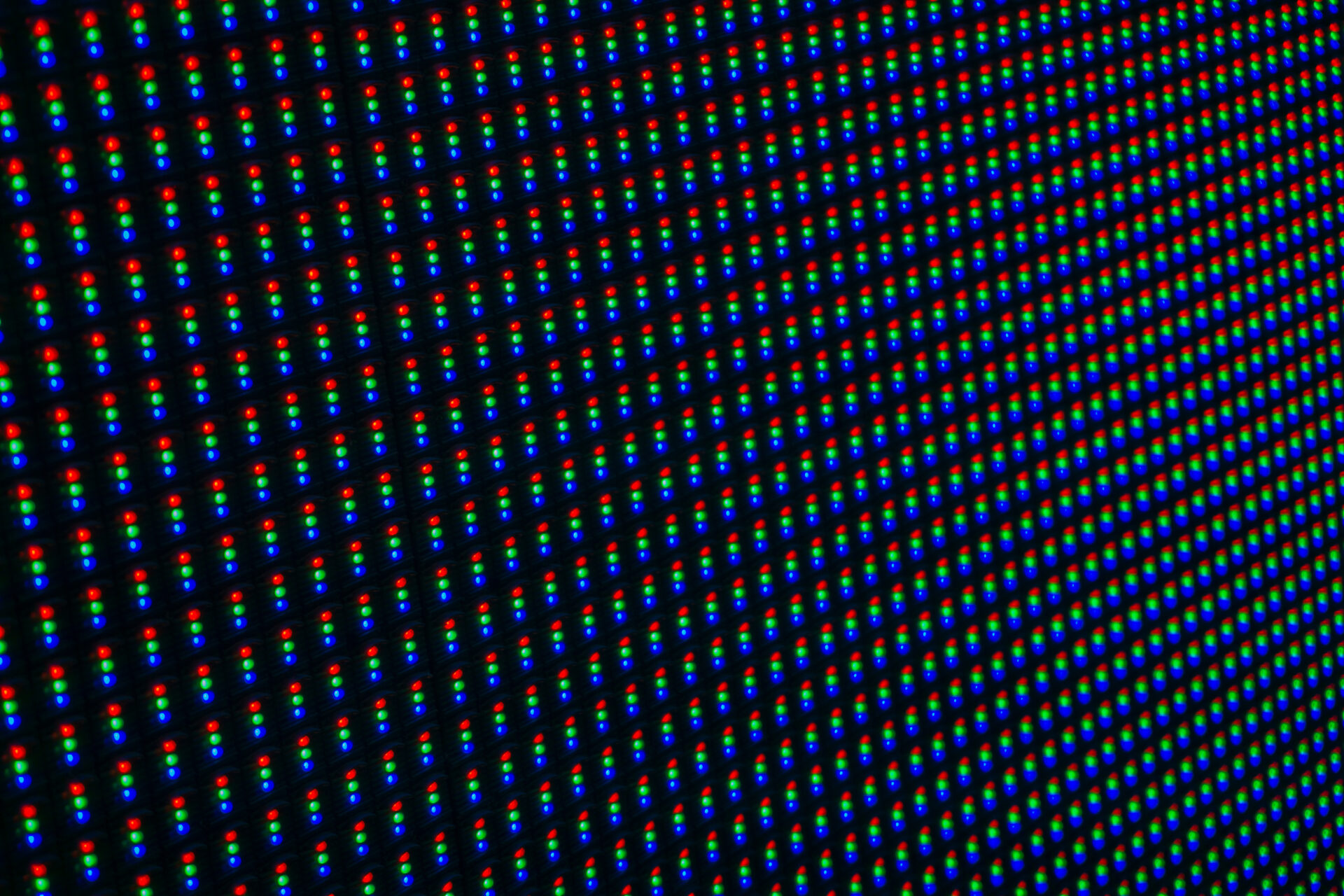
Micro LED chips are microscopic LED chips less than 0.1 millimeters in size. Display technology using these Micro LED chips takes smaller versions of the LEDs used as light sources in everyday lighting and traffic lights and arranges them across entire display panels. This allows displays to leverage LED’s characteristics of high brightness, low power consumption, and long lifespans while using the small LED chips to create detailed images.
Micro LED displays produce rich, painting-like images by precisely controlling the color and brightness of each pixel. This technology is based on the same principle behind the large screens seen in sports stadiums. But Micro LED displays use smaller individual light sources to produce highly detailed images viewable from a close distance. A Micro LED chip is less than half the size of a standard LED, and some are less than 1/6 of the size.
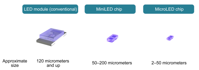
As the technology evolves, Micro LEDs are being considered for use in a wide range of devices such as digital signage, televisions, wearable devices, and augmented reality (AR) smart glasses. By enabling smaller and more sophisticated displays, Micro LED technology has the potential to contribute to significant advances in electronic devices.
Challenges for the practical application of Micro LED displays
There are, however, multiple obstacles to the widespread use of Micro LED displays.
One such obstacle is cost. The price tags of about 80,000 USD on an 89-inch display and about 150,000 USD on a 110-inch display launched in 2022 illustrate this. As of January 2024, a major South Korean electronics manufacturer sells Micro LED displays for TVs but the prices are still higher than the price range for the average consumer. The cost of the Micro LED chips themselves is one factor in the high prices, but it is thought that the lack of an established, efficient manufacturing process is also a factor. This may mean that manufacturing costs have not been reduced as much as expected.
Another big challenge is the LED arrangement process (mass transfer). When manufacturing a Micro LED display, more than 24 million red, green, and blue LED elements are necessary to form the more than 8 million pixels for a 4K display. A method called “pick and place” is used to position these LED elements on the circuit board. An elastomer stamp is used to pick up LED chips and transport them to the target location. There is a limit to the number of LED chips that can be moved at once, resulting in the problem of extremely long times required to move all of the chips.
Another bottleneck in the manufacturing process is low illumination rate and the repair of non-illuminating parts. The LED chips used to produce high-resolution images are so small that connection to the circuit board becomes difficult, leading to an increased trend in non-illumination. When an LED chip fails to illuminate, it leads to a pixel defect where it cannot show the correct color, or in the worst case a dead pixel. A partial repair is necessary to address the issue.
To take on these challenges, various manufacturers are developing assembly process technologies such as batch formation of LEDs on wafers and mass transfer of LED chips. Many other manufacturing approaches are also being tried. One is “tiling,” which arranges small LED displays like tiles to create one large display. Others involve sealing or laminating LED chips.
ArrayFIX can solve Micro LED display challenges
As Micro LED display technology continues to evolve, Dexerials provides products that can play important roles in Micro LED display manufacturing. In addition to products such as optical films and optical elastic resins, Anisotropic Conductive Film (ACF) is drawing attention as an indispensable part of electrically connecting various parts of the display. In particular, a particle-arrayed ACF called ArrayFIX was developed for the miniaturization of terminal connections such as those found on Micro LED chips, and its potential applications have been highly evaluated.
ArrayFIX technology for Micro LEDs
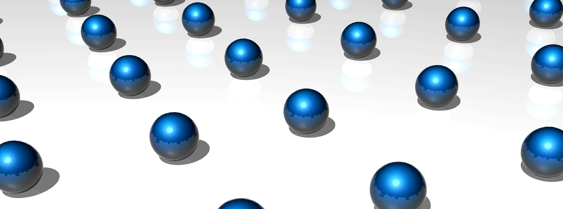
As the connection area between LED chips and substrate shrinks in the Micro LED display manufacturing process, Dexerials’ ArrayFIX continues to evolve to meet that challenge. Specifically, the diameter of conductive particles is smaller than in previous products, resulting in higher particle density that enables greater precision in positioning.
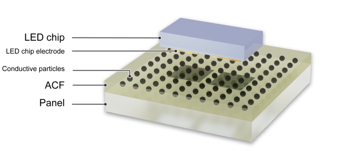
Previously, the highest density ArrayFIX ACF had a particle diameter of 3.2 micrometers and a particle density of 28 kpcs/mm2, designed for Chip on Glass (COG) technology to mount ICs for high-resolution displays such as those for smartphones. However, ArrayFIX for Micro LEDs requires even higher precision, so we are designing a version with particle diameter reduced to 2.2 micrometers and particle density increased to 58 kpcs/mm2.
ArrayFIX for Micro LEDs enables stable connections due to the arrayed particles and low-resistance connection to extremely small electrodes of 100 μm² and below. Additionally, because the particles maintain their positions, excellent insulation is provided even with extremely small distances between electrodes.
The use of ArrayFIX can simplify the manufacturing process by enabling processing at lower temperatures than those required for conventional solder bonding and removing the need for Au/Sn bump formation. Simply applying ACF to the substrate is all the preparation that is required. With less pre-processing needed compared to other bonding methods, significant time and cost savings can be expected. In addition, temporary fixing of LEDs during mass transfer is possible between room temperature and 50°C, followed by thermocompression bonding all at once later. This can increase the efficiency of large-scale display manufacturing.
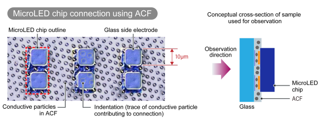
Innovative ACF placement technology for Micro LED display manufacturing
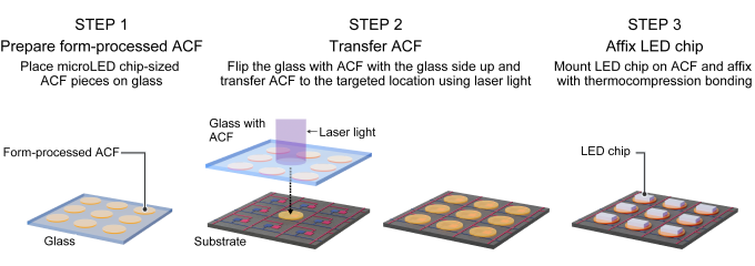
High-precision chip mounting is a critical factor in the Micro LED display manufacturing process, significantly influencing the final product’s quality. To take on this challenge, Dexerials has developed an innovative way to accurately place Pre-Cut ACF pieces in targeted locations. The key to this technology is micron-sized pieces of ArrayFIX.
To be specific, we devised technology to use lasers to transfer ACF only to places where mounting is required. This allows ACF placement only where it is needed to enable high-precision mounting of LED chips on the circuit board.
Other applications of this technology are also possible. We are considering a process to remove a specific LED chip and the ACF around it with a laser, transfer a new ACF piece to a targeted location, and repeat bonding. This has the potential to improve display quality and manufacturing efficiency.
In addition, this technology can make it possible to transfer ACF to only the substrate connection area. We are also exploring further applications such as the manufacturing of transparent Micro LED displays.
By leveraging these cutting-edge technologies, Dexerials will continue its technological development efforts to bring richness and convenience to everyone’s lives.
- SHARE
 Back to top
  Contact us


