- Elemental Technologies
Fundamentals of Sputtering
Contents
Principle of Sputtering
Technologies to form thin layers on the surface of film and glass substrates include coating, printing, plating, and vapor deposition.Sputtering is a technology used to form nano-level thin layers composed of metals and ceramics with a high purity and exact composition.
The illustration below depicts the image of sputtering in an easy-to-understand manner.A thin layer is formed by “throwing a stone into water (target) in a pool and making a splash to make the water (target) adhere to the substrate.
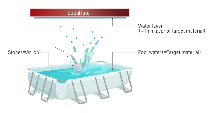
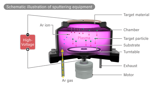
In actual sputtering, the “stone” is an inert gas such as argon (Ar) filled in a vacuum container (vacuum chamber).
The “puddle” in the above illustration is the material that forms the thin film, called the “target material,” such as metal or ceramic.
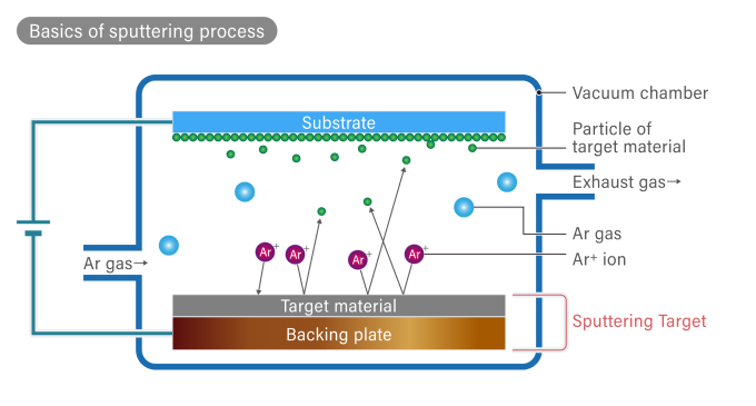
In sputtering, argon gas is introduced into a vacuum, and a negative voltage is applied to the target material to generate a glow discharge, which is also used in fluorescent lamps.
Argon ions, which become plasma with a positive charge, collide with the surface of the target material at ultra-high speed (approximately 3.2 km per second), violently bouncing off particles (atoms and molecules) in the target material.
The bounced particles vigorously adhere to the surface of the target material, and when they are deposited, a thin layer is formed.
This is the principle of sputtering.
Sputtering is being widely used in the electronics industry.
Compared to other technologies, thin layer deposition by sputtering has the following outstanding features.
-Dense and hard layers can be deposited.
-Composition can be precisely adjusted.
High-precision control of layer thickness
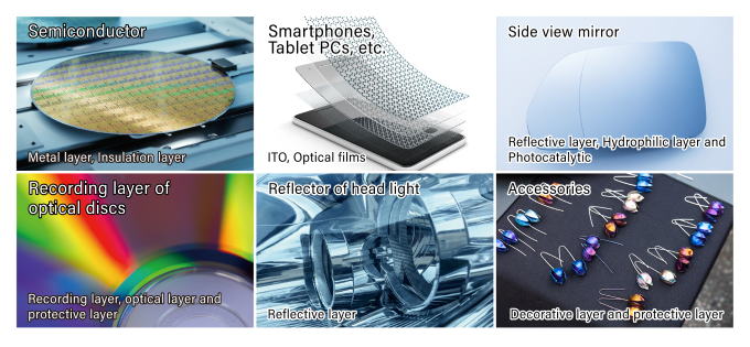
Taking advantage of these features, the technology is used for electronic products and materials such as metal layers, transparent conductive layers, optical films, and optical discs.
It is also applied in the production of automotive mirrors and accessories that beautifully reflect light because it can achieve a variety of optical properties through the formation of thin metal layers.
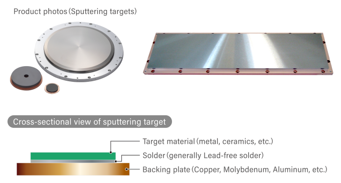
What is a sputtering target?
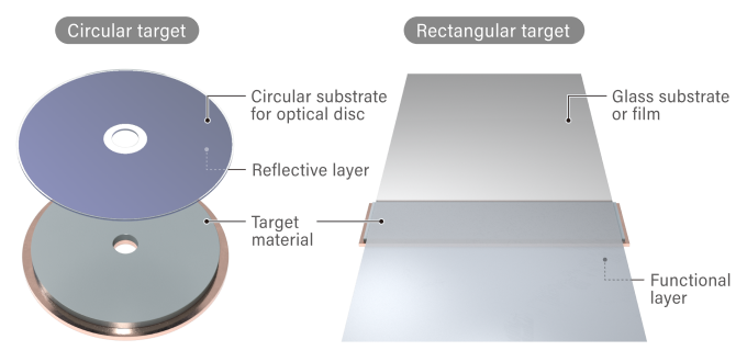
A sputtering target is a bulk material that serves as an “ingredient” for thin layers formed on a substrate.Various metals and ceramics are used depending on the type of thin layer, and circular or rectangular targets are used depending on the shape of the target substrate.Sputtering targets in the commercial are bonded by solder to backing plates made of copper, molybdenum, aluminum, etc., to facilitate installation in sputtering equipment.
Circular targets, shown in the figure on the left below, are used for the deposition of circular products such as semiconductor wafers and optical discs.
Rectangular targets are suitable for depositing large-area substrates such as glass and film. They are usually used for continuous deposition of glass and film moving over the target as shown in the illustration on the right below.
The illustration below is a cross-sectional image of the inside of an optical disc production system.
The target material is placed at the top of the chamber, and the optical disc to be deposited is placed on a turntable, where sputtering is performed.
The equipment has a “load lock mechanism,” so the disc can be replaced while maintaining a vacuum in the chamber.
Sputtering Technology Responding to Diverse Needs
The strength of Dexerials’ sputtering target is “the ability to mix a wide variety of elements to create the optimum composition for each purpose. To date, we have provided about 200 types of targets for prototypes and about 30 types for mass production.
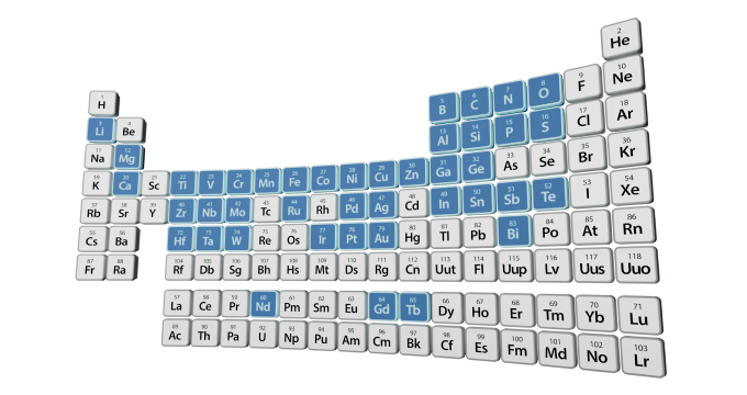
We have 40 different elements available for sputtering targets.
We only provide the “target material” for sputtering.
On the other hand, our greatest expertise lies in the technology to mix multiple metals, metal oxides, and other ceramic materials in optimum proportions for sputtering.
We will continue to provide functional thin layers based on this technology to meet our customers’ requirements.
- SHARE
 Back to top
Elemental Technologies Popular articles